
PRODUCTS
Product information
About export products
Hanwa Trading Co., Ltd. exports and sells semiconductor inspection equipment, electronics control equipment, etc. mainly to China.
We have a wide and deep network of local universities, research facilities, and semiconductor-related companies in China. While making full use of this network, we will accurately grasp the local needs, consider the differences in business practices and cultures between the two countries, consider product specifications, negotiate prices, delivery dates, etc., and act as a bridge with excellent Japanese manufacturers. increase.
As a trustworthy entity for both local end-users and Japanese manufacturers, we respond with speed and create added value for your business.
In addition, we also accept consultations on developing the Chinese market and expanding sales channels.
Please entrust Hanwa Trading Co., Ltd. with overseas trade business, including dealing with China.
Examples of main products handled (partial)
ESD (TLP/CDM/HBM) tester
ESD (Electro Static Discharge) failures in semiconductor chips account for more than 40% of product failures. So ESD test is one of the very important tests.

TLP (Transmission Line Pulse) Tester
: Characteristic inspection of ESD protection circuit
It tests the current and voltage of electrostatic protection circuits for semiconductor wafers and ICs with packaged chips, generates TLP curves and analyzes technical parameters.
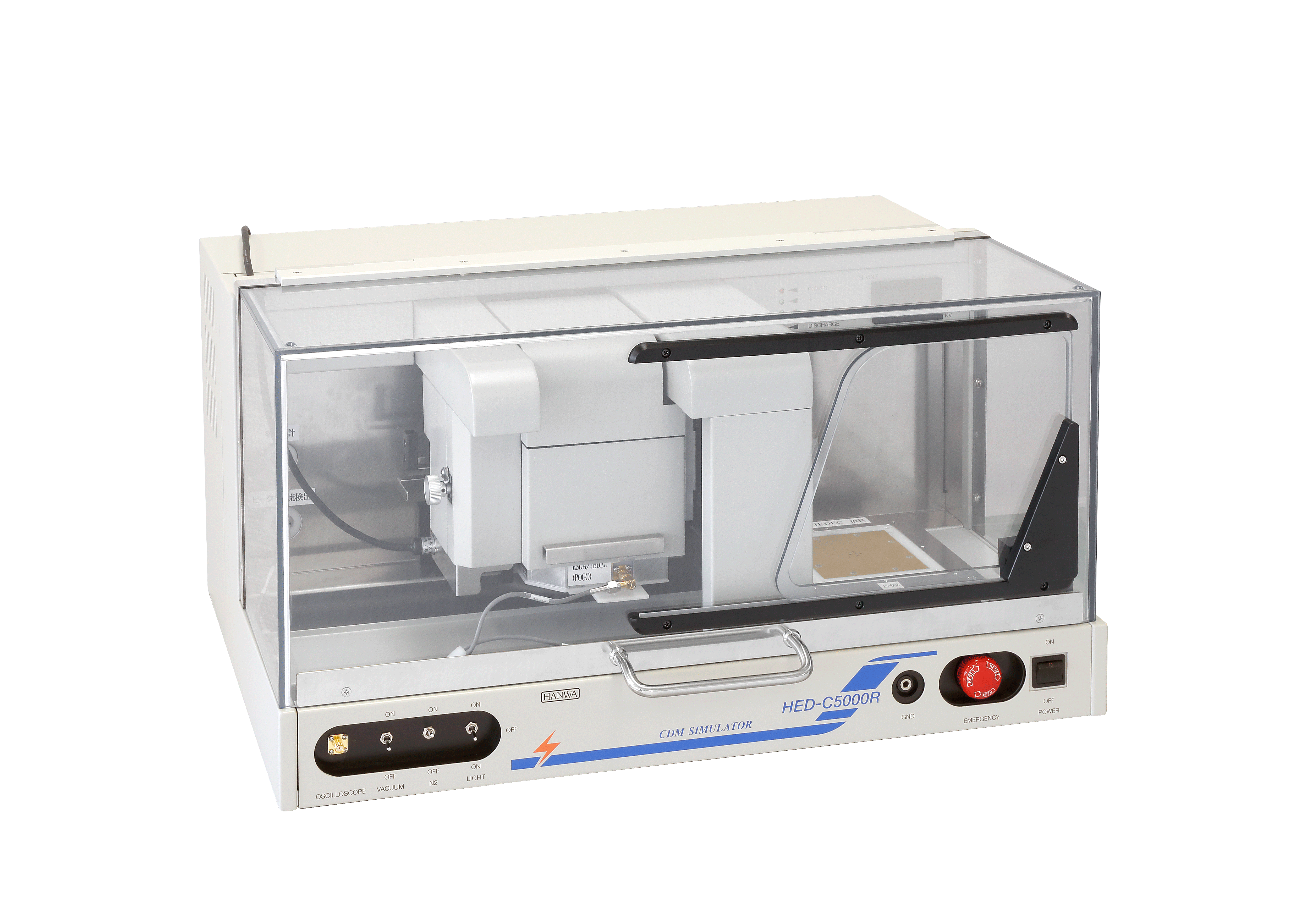
CDM tester
: Inspection of discharge capability of semiconductor parts in charging mode
The DUT or module is charged by direct/indirect charging method, and the electrostatic discharge phenomenon is simulated by contacting the object to be measured through the device's discharge needle. This tests whether there is damage or failure in the internal circuit or structure of the device under test.

HBM/MM/LATCHUPTester
: Human body mode/machine mode/latch-up test
Simulate the effects of human body discharge mode, machine discharge mode, and latch-up discharge mode on semiconductor devices at the package level to check for device failures, and define the breakdown tolerance level of the device according to the magnitude of the failure voltage. (Device maximum PIN: 2048PIN).

Compact ESD tester
For power device and low pin count ESD test
It also has a leak measurement function, and can perform destruction judgment by ESD only with this tester.
semiconductor curve tracer
By combining with a variety of units, it can be used for characterization in any process.


Supports the world's highest peak ultra-high voltage and large current
semiconductor curve tracer
Ideal for measuring the characteristics of various semiconductors such as IGBTs, MOSFETs, transistors, and diodes. Applied voltage and current waveforms can be observed as well as IV curves. The device has a maximum voltage of 15KV and a maximum current of 8KA, and can test anything from low power DIODE MOSFETs to higher power IGBTs.
By adding test conditions, change trends of static parameters such as VCE, VGE, and ID, and real-time waveforms of various parameters such as VF, IDSS, VTH, VDSON, and BV can be reproduced. At the same time, it can also be connected to a prober to test wafers.
ceramic package
Ceramic packages are generally used in fields with strict external environmental requirements. The reliability of the device depends on whether the whole system works properly and achieves the expected design effect.
Advantages of ceramic packages
(1) High moisture resistance and less microcracks
② Resistant to thermal shock tests and temperature cycle tests, and has high mechanical strength
③ Small coefficient of thermal expansion and high thermal conductivity
④ Excellent insulation and airtightness, chips and circuits are not affected by the surrounding environment
Wide range of support from customized packages to standard packages for device evaluation

PGA (Pin Grid Array)

LCC (Leadless Chip Carrier)

F/P (Flat lead package)

CMOS PKG
DC/AC Tester
We provide a system for testing DC parameters, AC parameters, thermal resistance, and L load of power devices (IGBT MODULE, MOSFET, TRANSISTOR, DIODE, SCR, REGULATOR, etc.).
It complies with MIL-STD-750 (standard for semiconductor discrete devices) and AQG324 (standard for European automotive power devices).

dynamic test system
Tests dynamic switching time, Trr time, short circuit current and RBSOA of power devices.

DC tester
Fully automatic mass production testing of power device parameters such as VF, VDSON, BVDSS, IDSS, IGSS, GMP, VP, VTH.

thermal resistance tester
The Power Device Transient Thermal Resistance Tester tests changes in VF, VDS, VCE, and VGE before and after heating a power device, and evaluates the heat dissipation capability of the device based on the amount of voltage change.

thermal resistance tester
It is possible to test the thermal resistance and heat dissipation capability of ICs and discrete devices, analyze the internal structure of the device from the test results, and measure the device's K factor, thermal resistance curve, etc. There are two measurement methods: fixed temperature and fixed power.

Thermal Resistance/Power Cycle Tester
Upgrade from a thermal resistance tester to power cycle test up to 12 power devices simultaneously with test current up to 3600A. Measure the amount of change in VF/VCE/VGE voltage and calculate Rth. The structure function generates change curves for thermal resistance and heat capacity inside the device to determine product failure mechanisms under different conditions.
It is the only product in the industry that can be used for active power cycle testing.
others

Nickel alloy processed product (foil material)
Nickel has high strength at high temperatures, and has excellent corrosion resistance to seawater, freshwater, and aqueous solutions of neutral and alkaline salts. In addition, nickel alloys with alloying elements are highly resistant to oxidation.
Nickel alloys can be cold-rolled, hot-rolled, drawn, and forged, so they are effective in workability and are widely used in industrial fields such as industrial machinery and semiconductor manufacturing equipment.

Sapphire processed product
Single-crystal sapphire has excellent hardness, heat resistance, thermal conductivity, and chemical resistance, and stably transmits a wide range of light from the ultraviolet to mid-infrared regions, making it very suitable for semiconductor devices and optical equipment. used a lot.
Typical applications for the semiconductor industry include process monitoring windows in semiconductor manufacturing equipment, wafer transfer lifts inside these equipment, probe pins, and tubular processed products for flowing highly corrosive chemicals and gases. And so on.

半導体検査装置用対物レンズ
対物レンズは半導体検査装置やレーザー微細加工におけるキーデバイスです。
特にNA(開口数)や集光スポット径は、レンズが搭載される装置のパフォーマンスに大きく影響します。

エアベアリング(静圧空気軸受)
エアベアリングは外部より圧縮空気を軸受すきまに送り、その圧力によって負荷能力を発生する軸受けです。軸と軸受は完全非接触のため以下のような特徴があります。
-
スティックスリップがなく、滑らかに回転、精度は半永久的に維持
-
潤滑油を使用せず、クリーンでメンテナンスフリー
-
摩擦による発熱がなく高速・高加速に最適

偏光ビームスプリッタ (PBS)
偏光ビームスプリッター(PBS)は、S偏光(平行偏光)とP偏光(垂直偏光)の光を効率的に分離することができます。S偏光は光波が入射面に平行に振動する偏光であり、P偏光は入射面に対して垂直に振動する偏光です。
PBSは二つの偏光成分を分離することで、特定の�偏光状態を有する光のみをターゲットとする高度な光学操作を可能にし、光学研究や様々な技術応用に不可欠な役割を果たします